
PCBAvailable
PCB Trace Width Calculator
Estimate trace width, resistance, voltage drop, and power loss using IPC-2221 equations.
Calculator category
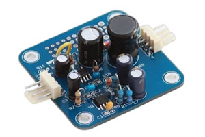
PCB calculators help translate circuit requirements into manufacturable board geometry and layout constraints. They support trace sizing, via current estimates, copper thickness decisions, and thermal design checks that matter in hardware design, power routing, and troubleshooting board-level reliability issues.
Available Calculators
10
Engineering Applications
4
Each listed tool links to a working calculator with engineering inputs, formulas, examples, notes, and related resources.
Estimate trace width, resistance, voltage drop, and power loss using IPC-2221 equations.
Estimate trace ampacity, resistance, voltage drop, and power loss using IPC-2221 equations.
Convert copper weight and thickness units and calculate trace cross-sectional area.
Estimate plated via resistance, current sharing, voltage drop, power loss, and loading risk.
Calculate temperature-adjusted trace resistance, voltage drop, power loss, and rail loss percentage.
Estimate plated thermal-via conductance, parallel thermal resistance, heat flow, and temperature difference.
Estimate preliminary surface creepage from working voltage, pollution degree, CTI group, and insulation type.
Estimate required air clearance, reverse-check voltage bands, and validate an existing PCB gap.
Estimate single-ended and differential impedance for coupled microstrip or stripline routing.
Estimate single-ended impedance, effective dielectric constant, propagation velocity, and delay.
Choose the calculator that matches the decision you need to make: decode a component marking, size a value, check a frequency response, estimate loss, or verify a safety margin. A category page is useful only when it helps you reach a working tool, so this page lists released calculators only.
Calculator results depend on unit choices, idealized formulas, tolerance, temperature, frequency range, and component limitations. Review the formula and engineering notes on each calculator page before using the result in a schematic, BOM, or PCB layout.
Use the calculated value as a design reference, then confirm it against datasheets, derating curves, layout parasitics, measurement conditions, and manufacturer limits. The related guides below provide background when a calculation needs more context.
Engineering Guide
Carry differential impedance geometry into a complete routed channel with reference-plane continuity, intra-pair skew, transition symmetry, and measured validation.
10 min · Advanced
Engineering Guide
Understand PCB trace width, current capacity, copper thickness, temperature rise, trace resistance, voltage drop, I²R power loss, IPC-2221-style estimates, IPC-2152 guidance, and practical high-current routing checks.
22 min · Intermediate
Engineering Guide
Learn how PCB via diameter, plating thickness, board thickness, resistance, current density, parallel via arrays, voltage drop, I²R heating, thermal vias, and stackup affect reliable high-current via design.
21 min · Intermediate
Engineering Guide
Design controlled-impedance PCB traces using the ECParts microstrip, stripline, and differential-pair models with practical stackup and fabrication boundaries.
18 min · Intermediate
Engineering Guide
Design PCB creepage and clearance using insulation coordination, working and impulse voltage, pollution degree, CTI, altitude, manufacturing constraints, and verification boundaries.
18 min · Intermediate
Power electronics calculators for regulators, converters, thermal design, current estimates, and hardware margins.
Open →MOSFET calculators for switching loss, conduction loss, gate drive, thermal checks, and power hardware design.
Open →Use electronics conversion tools for frequency and period, AWG wire gauge, dBm and watts, hexadecimal, decimal, binary, and engineering workflows.
Open →